If you are looking for high-quality products, please feel free to contact us and send an inquiry, email: brad@ihpa.net
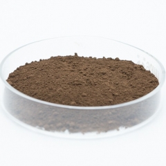
Nano Silicon is a super-fine powder of crystalline silicon with small particle size, large specific surface area, high activity, and low loose density. It has a wide gap energy semiconductor and is also a high-power light source material.
Nano silicon can be used in a wide variety of applications in nanotechnology, including micro- and nanoelectronics, sensors, biotechnology, chemical and filtration industries, etc. The tunable properties of these nanostructured materials have opened new pathways for fabrication of highly sensitive, miniaturized and cost effective devices.
In addition to their versatile nanostructures, these materials are also characterized by their tunable pore sizes, porosity, thermal and mechanical properties, optical and electrical properties, biocompatibility, and compatibility with microelectronics. Porous silicon obtained by electrochemical etching of polished silicon is a versatile material for nanotechnology due to its tunable pore size, porosity, thermal and mechanical properties, and other features.
The tunable pore size and porosity of porous silicon can be modified by band gap engineering, composites, or core shell structures to enhance their performance in different application areas. Moreover, porous silicon is compatible with microelectronics for fabrication of high-density and high-performance devices.
Silicon is the basic material for most integrated circuits and electronics. Its discovery in the 1970s revolutionized the field of silicon based semiconductor technology and led to the development of semiconductor devices that are widely used in everyday products. However, it took decades to understand the properties of single crystal silicon and its underlying semiconductor technology. Today, nanotechnology allows incredibly detailed nanoscale etching, down to 10 nanometers on a silicon wafer.