If you are looking for high-quality products, please feel free to contact us and send an inquiry, email: brad@ihpa.net
What is it?
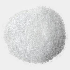
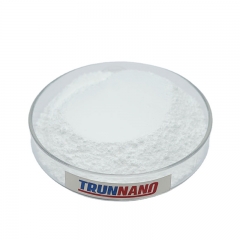
Gallium Nitride Powder
?
Gallium Nitride is an inorganic compound with the chemical formula GaN. It is a mixture of nitrogen and galium. It is a direct bandgap silicon and has been widely used in light emitting diodes ever since 1990. This compound exhibits a wurtzite like structure and high hardness. The energy gap for gallium nitride, 3.4 electrons per second, is extremely wide. This allows it to be used in high power, high speed optoelectronic components. Gallium nitride is a good choice for violet laser diodes. It can also be used in nonlinear semiconductor-pumped, solid-state lasers.
The key features of Gallium Nitride Powder
GaN is a very stable and hard melting material. Its melting point is approximately 1700 degC. GaN exhibits the highest degree of ionization (0.5 to 0.43) of all III-V compounds. GaN crystals are hexagonal wurtzite structures at atmospheric pressure. It contains 4 atoms in a cell and has an atomic volume about half of that of GaAs. It’s a great coating protection material because of its high hardness.
1. Chemical properties
At room temperature, GaN can dissolve in water, acids, bases and hot alkaline solutions. However, it is insoluble at room temperature. For defect detection of low quality GaN crystals, NaOH and H2SO4 can quickly corrode the GaN. GaN has unstable properties at high temperatures and is more stable under N2 gas than HCL or hydrogen.
2. The electrical characteristics
The device’s electrical properties are key factors. Intentionally doped GaN in all cases is n-type. At 4×10¹⁶/cm3, the electron concentration of best samples is around 4. Preparations of P-type specimens are usually highly compensated. Research in this area has been conducted by many groups. Nakamura was one of them. He reported that the highest mobility data for GaN were mn=600cm2/v*s (at room temperature) and mn=1500cm2/v*s (at liquid nitrogen temperature). The corresponding current carrying Subconcentrations are n=4×10¹⁶/cm3 or n=8×10¹⁵/cm3. In recent years, the electron concentration values for MOCVD-deposited GaN sheets are reported at 4 x 10¹⁶/cm3, and 1016/cm3 respectively. The results of plasma activated MBE are 8x 10³/cm3, and 1017/cm3. The undoped carrier can be controlled within the range of 1014-1020/cm3. Additionally, the P-type process, thermal annealing and Mg low energy electron beam irradiation have allowed for the control of the doping level to be controlled at 1011-1020/cm3.
Gallium Nitride Powder’s applications
GaN material series can be used to develop high-temperature and high power electronic devices. Many GaN heterostructures can now be grown thanks to MBE technology, breakthroughs in thin-film growth technologies and progress in the application of GaN material. GaN material was used to create new devices, such as the Metal Field Effect Transistor(MESFET), Heterojunction Field Effect Transistor(HFET), Modulation Doped Field Effect Transistors (MODFET), and others. The AlGaN/GaN structure, which has been modulation-doped, has high electron mobility (2000cm2/v*s), high saturability (1x107cm/s), low dielectric constant and is preferred for making microwave device; GaN. The substrate’s band gap is 3.4eV and sapphire, which allows the device to work under high power conditions.
Gallium Nitride powder supplier
Tech Co., Ltd. () is a professional nitride powder Over 12 years’ experience in chemical products development and research. We accept credit cards, T/T and West Union payments. We will ship goods overseas via FedEx, DHL and by air or sea to our customers.
You can find high-quality powdered boron carbide here Please contact us Send an inquiry
Gallium Nitride is an inorganic compound with the chemical formula GaN. It is a mixture of nitrogen and galium. It is a direct bandgap silicon and has been widely used in light emitting diodes ever since 1990. This compound exhibits a wurtzite like structure and high hardness. The energy gap for gallium nitride, 3.4 electrons per second, is extremely wide. This allows it to be used in high power, high speed optoelectronic components. Gallium nitride is a good choice for violet laser diodes. It can also be used in nonlinear semiconductor-pumped, solid-state lasers.
The key features of Gallium Nitride Powder
GaN is a very stable and hard melting material. Its melting point is approximately 1700 degC. GaN exhibits the highest degree of ionization (0.5 to 0.43) of all III-V compounds. GaN crystals are hexagonal wurtzite structures at atmospheric pressure. It contains 4 atoms in a cell and has an atomic volume about half of that of GaAs. It’s a great coating protection material because of its high hardness.
1. Chemical properties
At room temperature, GaN can dissolve in water, acids, bases and hot alkaline solutions. However, it is insoluble at room temperature. For defect detection of low quality GaN crystals, NaOH and H2SO4 can quickly corrode the GaN. GaN has unstable properties at high temperatures and is more stable under N2 gas than HCL or hydrogen.
2. The electrical characteristics
The device’s electrical properties are key factors. Intentionally doped GaN in all cases is n-type. At 4×10¹⁶/cm3, the electron concentration of best samples is around 4. Preparations of P-type specimens are usually highly compensated. Research in this area has been conducted by many groups. Nakamura was one of them. He reported that the highest mobility data for GaN were mn=600cm2/v*s (at room temperature) and mn=1500cm2/v*s (at liquid nitrogen temperature). The corresponding current carrying Subconcentrations are n=4×10¹⁶/cm3 or n=8×10¹⁵/cm3. In recent years, the electron concentration values for MOCVD-deposited GaN sheets are reported at 4 x 10¹⁶/cm3, and 1016/cm3 respectively. The results of plasma activated MBE are 8x 10³/cm3, and 1017/cm3. The undoped carrier can be controlled within the range of 1014-1020/cm3. Additionally, the P-type process, thermal annealing and Mg low energy electron beam irradiation have allowed for the control of the doping level to be controlled at 1011-1020/cm3.
Gallium Nickel GaN powder CAS 25617-97-4
GaN material series can be used to develop high-temperature and high power electronic devices. Many GaN heterostructures can now be grown thanks to MBE technology, breakthroughs in thin-film growth technologies and progress in the application of GaN material. GaN material was used to create new devices, such as the Metal Field Effect Transistor(MESFET), Heterojunction Field Effect Transistor(HFET), Modulation Doped Field Effect Transistors (MODFET), and others. The AlGaN/GaN structure, which has been modulation-doped, has high electron mobility (2000cm2/v*s), high saturability (1x107cm/s), low dielectric constant and is preferred for making microwave device; GaN. The substrate’s band gap is 3.4eV and sapphire, which allows the device to work under high power conditions.
Gallium Nitride powder supplier
Tech Co., Ltd. () is a professional nitride powder Over 12 years’ experience in chemical products development and research. We accept credit cards, T/T and West Union payments. We will ship goods overseas via FedEx, DHL and by air or sea to our customers.
You can find high-quality powdered boron carbide here Please contact us Send an inquiry